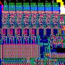
Hallo Besucher, der Thread wurde 8,3k mal aufgerufen und enthält 55 Antworten

letzter Beitrag von androSID am

REU Controller 8726R1 dissection...

  • 18) D0


    D0..D7 is the C64\C128 data bus.


    D0io..D7io is the bidirectional data bus inside the 8726 related to D0..7.


    D0..7 drivers\buffers have identical chip layout, so we just focus on D0.


    ;---


    On the input side, D0 is sampled with a transparent latch during PHI2.


    The output of the latch is placed on the D0io bus by a non_inverting buffer

    controlled by OE_DI# (low active), which is generated in "3) CS#".


    ;---


    On the output side, we have a non_inverting driver fed by D0io, driving D0,

    controlled by OE_D (high active), which is generated in "3) CS#".


    Drivers have output FETs switching non_overlapping to GND\VCC

    it's a variation of the driver we already had in "5) rw",

    making creative use of a RS flipflop built from two NOR gates.


  • 20) A0..A15 NOR


    First, we have a 16 input NOR gate, which gives out high on C64is$FF00 (high active) if A0..15 is $FF00.


    Basically said NOR gate is a metal trace which passes by all of the A0..A15 drivers\buffers.

    North of the A0 driver\buffer, a ca. 10kOhms pullup resistor (FET) ties said metal trace to VCC.


    Each of the A0..7 buffers contains a FET switching said metal trace to GND if a A0..7 address line is not low.

    Each of the A8..15 buffers contain a FET switching said metal trace to GND if a A8..15 address line is not high.


    ;---


    Second, we have a lump of logic at the West side of the chip, "between" D0 pad and A15 pad.


    C64is$FF00 goes through an inverter, then into a NOR gate together with R/Wi# (which is low when the 6510 does a memory write).

    The output of that NOR gate (which goes high when there is a 6510 write to $FF00) is sampled by a transparent latch during PHI2.

    The output of said latch goes through an inverter, is sampled by another transparent latch during PHI1,

    goes through a non_inverting super buffer and becomes C64was$FF00w.


    So if there was a 6510 write to $00FF in the previous PHI2_in cycle,

    C64was$FF00w (high active) goes high in the current PHI2_in cycle.


    C64was$FF00w goes to the DMA start logic in "31) tapeworm from hell".


  • 21) RAS_CAS_logic


    It is located North East in the chip, close to the CAS1#,CAS0#,RAS1#,RAS0# pads.


    It generates the signals for these parts, as well as the control signals for the MA0..8 multiplexers,

    also it generates the signals DMA1 and OED_GATE.


    8726 does DMA DRAM acceess during PHI2_in is low, and DRAM refresh during PHI2_in is high.


    Note:

    The VIC-II generates the PHI0 clock by dividing DotClock by 8,

    the 6510 generates PHI2 (for the Expansion Port, the SID and the two 6526 chips) from PHI0.

    PHI2 changes with the rising edge of the DotClock.


    ;---


    To make it short:

    anything timing related running with the dot clock (faster than PHI2_in, that is) is located in that area of the chip.


    DotClk# goes into a clock generator which is built around a RS flipflop containing two NOR gates (that's standard).

    That clock generator gives us two non_overlapping clock signals, Dot and Dot#.


    A falling edge detector (clocked by Dot\Dot#) sets a two Bit counter (clocked by Dot\Dot#) to $01 after the falling edge of PHI1.

    ;

    Bit 0 of the counter goes through an inverter, and becomes OED_GATE.

    Bit 0 also enters another clock generator (synchronized with Dot#) (another RS flipflop containing two NOR gates),

    which gives us the two non_overlapping clock signals OEDG and OEDG#.

    ;

    Bit 1 gives us the signal DMA1.


    We have two rising edge detectors (clocked with OEDG\OEDG#), scanning the refresh0 and refresh1 signals from "22) refresh counter",

    generating RAS0o# and RAS1o# for DRAM refresh.

    Note, that refresh0 and refresh1 never are high at the same moment.


    We have a falling edge detector (clocked with OEDG\OEDG#), which scans PHI2 (synchronized with OED_GATE),

    generating RAS0o# and RAS1o# during DMA (when DMAo# is low) according to the two bank select signals

    AM_bank0 and AM_bank1 [see "26) bank select logic"].

    Note, that AM_bank0 and AM_bank1 never are high at the same moment.


    The multiplexer for AM0..8 [see "13) MA8"] sets AM_refresh to high by default, what turns AM_lo and AM_high to low,

    so that AM0..8 are fed by the DRAM refresh counter.


    If there is an active DMA (DMAo# is low), some timing circuity fed by PHI2 turns AM_refresh low,

    and sets MA_lo as well as MA_high to high in the right moment, making sure that the lower/higher part of the AM0..17 address

    is passed through MA0..8 to the DRAMs according to the RAS#\CAS# sequence.


    Said timing circuitry also enables CAS0o# and CAS1o# according to the bank select signals AM_bank0 and AM_bank1

    (which are synchronized with OED_GATE).


    ;---


    The RAS_CAS_logic is quite a tapeworm, and it doesn't fit on the screen.

    For navigating it, my orientation when starting to dissect it was the shape of the diffusion GND polygons in the East of the RAS_CAS_logic,

    so the odd red pattern in the first two schematics is a simplified form of that shape.


    Frank and me checked twice, if the polygonized picture really matches the microscopic picture of the silicon,

    and to us it does.


    ;===

  • To be on the safe side, Frank kindly did a simulation of my simplified RAS_CAS_logic,

    and to me and Frank the results of the simulation seems to match the oscilloscope pictures.


    Those want to know more in detail can view the simulation results with GTKWave:


    simulation_results.zip


    ;===


    Now for some oscilloscope pictures which Frank had made from a working 8726 chip:


  • 22) refresh counter.


    We have a 4 Bit prescaler, running at PHI2_in speed.

    It features the usual inverting\non_inverting ripple carry mechanism,

    but the counter Bits are stored in inverted form.


    A NOR gate detects, if the prescaler reached 15.

    The output of the NOR gate goes into sort of a shift register (clocked with PHI1\PHI2),

    with some edge detectors attached to it.


    The sequence goes like this:

    When the prescaler reached 15,

    in the next PHI2_in cycle it is set to 0, and refresh0 goes high.

    In the following PHI2_in cycle, refresh0 goes low, and refresh1 goes high.

    In the PHI2_in cycle after that, refresh1 goes low, and the refresh counter increments.


    In "21) RAS_CAS_logic", the RAS0o# and RAS1o# signals for DRAM refresh

    are generated from refresh0 and refresh1.


    The refresh counter is pretty much standard,

    except that TEST clears the refresh counter and the prescaler.


    //I think that the TEST signal was used for testing the chip at the factory.


  • 23a) D<>DD transfer latch


    D0io..D7io is the internal data bus which is related to C64\C128 memory data.

    DD0io..DDiio is the internal data bus which is related to the REU DRAM data (DRAM chips attached to the 8726, that is).


    When moving/swapping/comparing data between C64\C128 memory and REU DRAM memory,

    D<>DD transfer latch does temporarily store that data,

    also it contains the comparator.


    DRAM data access happens during PHI2_in is low,

    and C64\C128 data is valid during PHI2_in... if the VIC-II inside the C64\C128 allows this, of course.


    Actually, there are two latches, one for D>DD transfer, the other for DD>D transfer.


    Compare is done with one XOR gate per Bit.

    The XOR gates feed an 8 input NOR gate, which gives out EMP_EQ (high active) high

    if the constants of both latches are equal.


    Note, that CLR_TF clears the latches after a DMA is completed.


    ;---


    23b) compare logic


    Compare logic is located East of the D<>DD transfer latch.


    Basically, the comparator output has to be ignored if there is no DMA active,

    OR if the VIC-II has taken over the bus (holding/disrupting a DMA sequence),

    OR if the 8726 Register $01 is not set to VERIFY mode (for comparing a block of data).


    If the comparator output is not ignored, then a compare error will set Bit 5 in status Register $00,

    and CMP_ERR# tells the DMA control circuitry in "31) tapeworm from hell" that there was a compare error,

    to stop comparing, and to abort the DMA sequence.


  • 24) A0..15 address counter


    It is located South west in the chip, close to the A0..15 pads.


    And it generates A0..15 for C64\C128 memory access.


    We have two 8 Bit Registers for C64\C128 memory address,

    Register $02 for A0..7, Register $03 for A8..15.

    Registers are cleared during RESET.


    When the 6510 writes one of these registers, or when there is a RESET,

    the contents of both registers are transferred into the A0..15 counter.


    When the 6510 reads one of these registers,

    it actuall reads the contents of the A0..15 counter.


    ;---


    Special case:

    If RELOAD is enabled (Bit 5 in command Register $01 is set),

    the contents of the $02 and $03 Registers are reloaded

    into the A0..15 counter after completion of a DMA sequence.


    To be more precise:

    Register $01 Bit 5 goes into "31) tapeworm from hell",

    which generates the UPDATE signal, telling the counter control circuitry

    to reload the 16 Bit counter from the $02 and $03 Registers.


    ;---


    A0..15 counter features the usual inverting\non_inverting ripple carry,

    plus an 8 Bit carry lookahead mechanism.


    Counter Bits change with PHI2.


    "31) tapeworm from hell" enables counting with the cntA_CEN# signal (low active).

    If cntA_CEN# is low, A0..15 counter increments.


  • 25) transfer counter, N0..15


    It is located East of the "24) A0..15 address counter",

    and it contains the number of Bytes to be transferred during a DMA sequence.

    Means, it's a down counter.

    Besides that, the game is somewhat similar to what we had in the A0..15 address counter.


    We have two 8 Bit Registers for the amount of Bytes remaining to be transferred,

    Register $07 for N0..7, Register $08 for N8..15.

    Registers are set to -1 during RESET.


    When the 6510 writes one of these registers, or when there is a RESET,

    the contents of both registers are transferred into the transfer counter.


    When the 6510 reads one of these registers,

    it actuall reads the contents of the transfer counter.


    ;---


    Special case:

    If RELOAD is enabled (Bit 5 in command Register $01 is set),

    the contents of the $07 and $08 Registers are reloaded

    into the transfer counter after completion of a DMA sequence.


    To be more precise:

    Register $01 Bit 5 goes into "31) tapeworm from hell",

    which generates the UPDATE signal, telling the counter control circuitry

    to reload the 16 Bit counter from the $07 and $08 Registers.


    ;---


    Transfer counter features the usual inverting\non_inverting ripple carry,

    plus an 8 Bit carry lookahead mechanism.


    Also, we have NOR gates and two NAND gates, which tell "31) tapeworm from hell",

    that only two Bytes (cntN_is$0002#, low active) are remaining to be transferred by DMA,

    or that only one Byte (cntN_is$0001#, low active) is remaining to be transferred by DMA.


    //You probably don't want to transfer just one or two Bytes of data per DMA, do you ?


    Counter Bits change with PHI2.


    "31) tapeworm from hell" enables counting with the cntN_CEN# signal (low active).

    If cntN_CEN# is low, the transfer counter decrements.


  • 26) AM0..18 address counter


    It breaks into two parts:

    AM0..15 counter is located East from "25) transfer counter", not far from the MA0..7 pads.

    AM16..18 counter is located East from the status Register $00, not far from the MA8 pad.


    It generates the address for the REU DRAM, and selects one of the two DRAM banks.


    ;===


    For the AM0..15 counter, the game is pretty similar to what we had in "24) A0..15 address counter".


    We have two 8 Bit Registers: Register $04 for AM0..7, Register $05 for AM8..15.

    Registers are cleared during RESET.


    When the 6510 writes one of these registers, or when there is a RESET,

    the contents of both registers are transferred into the AM0..15 counter.


    When the 6510 reads one of these registers,

    it actually reads the contents of the AM0..15 counter.


    ;---


    Special case:

    If RELOAD is enabled (Bit 5 in command Register $01 is set),

    the contents of the $04 and $05 Registers are reloaded

    into the AM0..15 counter after completion of a DMA sequence.


    To be more precise:

    Register $01 Bit 5 goes into "31) tapeworm from hell",

    which generates the UPDATE signal, telling the counter control circuitry

    to reload the 16 Bit counter from the $04 and $05 Registers.


    ;---


    A0..15 counter features the usual inverting\non_inverting ripple carry,

    plus an 8 Bit carry lookahead mechanism that enables incrementing Bit 8..15 if there was an overflow in Bit 0..7,

    enabling _another_ 8 Bit carry lookahead mechanism that increments Bit16..18 if there was an overflow in Bit 0..15.


    Counter Bits change with PHI2.


    "31) tapeworm from hell" enables counting with the cntAM_CEN# signal (low active).

    If cntAM_CEN# is low, AM0..15 counter increments.


    ;===


    For the AM16..18 counter (that's three Bits), the game is a little bit different.


    We have one 3 Bit Register: Register $06 for AM16..18.

    Register is cleared during RESET.


    When the 6510 writes Register $06, or when there is a RESET,

    the contents of Register $06 are transferred into the AM16..18 counter.


    When the 6510 reads Register $06,

    it actually reads the contents of the AM16..18 counter.


    ;---


    Special case:

    If RELOAD is enabled (Bit 5 in command Register $01 is set),

    the contents of the $06 Registers are reloaded into the AM16..18 counter

    after completion of a DMA sequence.


    To be more precise:

    Register $01 Bit 5 goes into "31) tapeworm from hell",

    which generates the UPDATE signal, telling the counter control circuitry

    to reload the 3 Bit counter from the $06 Registers.


    ;---


    AM16..18 counter features the usual inverting\non_inverting ripple carry,

    counter Bits change with PHI2.


    ;===


    Now for the DRAM bank select logic attached to the AM16..18 counter.

    For AM16 and AM17, it reads the buffered counter outputs.

    For Bit 18, it directly and unbuffered taps into the AM18 counter Bit.


    BS (high active) goes through an inverting super buffer and becomes BS# (low active),

    defining the size of the two DRAM banks attached to the 8726 inside the REU,

    see "9) BS".


    Note, that we are just talking about the configuration of the 8726 bank select logic here,

    not about the _real_ size of a DRAM bank which physically is attached to the 8726.


    ;---


    BS=low (BS#=high): two banks with 256kB of DRAM each.


    if AM18=0, AM_bank1 goes high, selecting DRAM bank1.

    if AM18=1, AM_bank0 goes high, selecting DRAM bank0.


    Also, if the AM16..18 counter was 7 and rolls over to 0,

    it is cleared by AMB_CLR (to me, this looks redundant).


    ;---


    BS=high (BS#=low): two banks with 64kB of DRAM each.


    if AM16=0, AM_bank0 goes high, selecting DRAM bank0.

    if AM16=1, AM_bank1 goes high, selecting DRAM bank1.


  • 27) Register $01


    Located between A14 pad and MA8 pad, East of the A14 pad.


    Command register $01:

    Bit 0..1: transfer type. $0=C64>REU, $1=REU>C64, $2=SWAP, $3=VERIFY.

    Bit 2..3: present, but unused.

    Bit 4: 1=disable $FF00w decode.

    Bit 5: 1=enable AUTOLOAD. //enable reloading counters from Registers after completion of DMA sequence

    Bit 6: present, but unused.

    Bit 7: EXECUTE, 1=initiate DMA transfer per current config.


    Circuitry for the Register Bits is pretty much standard.


    A RESET sets Bit 4, and clears all of the other Bits.


    Bit 4 is set and Bit 7 is cleared with CLR_TF (high active) after completion of a DMA sequence.

    CLR_TF is generated in "31) tapeworm from hell".


    Bit 5 and Bit 7 are sampled with PHI1 in transparent latches

    before they go in low active form into "31) tapeworm from hell":

    R$01.Q5# and R$01.Q7.


    Bit 4 is sampled with PHI1 in a transparent latch and goes into "31) tapeworm from hell" as R$01.Q4 (high active),

    and there is an edge detector (clocked with PHI2) attached to R$01.Q4, generating R$01.Q42#.

    ;

    My guess is, that it goes like this:

    If Bit 4 is cleared, setting Bit 7 instantly initiates DMA transfer.

    If Bit 4 is set, setting Bit 7 makes the 8726 wait until the 6510 writes $FF00, than a DMA transfer is initiated.

    The edge detector seems to block the $FF00 detection from the previous PHI2_in cycle when Bit 4 goes from low to high.


    Bit 0 and Bit 1 go into a 2 Bit decoder (think of 74138 or 74139), which tells "31) tapeworm from hell" what to do:

    R$01.Y0 (high active) =high: C64>REU

    R$01.Y1 (high active) =high: REU>C64

    R$01.Y2 (high active) =high: SWAP

    R$01.Y3 (high active) =high: VERIFY

    //only one of these 4 signals can be high at a time.


  • 28) Register $0A


    Located between A14 pad and MA8 pad, East of Register $01.


    Address control Register $0A:

    Bit 0..5: not present, reads -1.

    Bit 6: 1=block AM0..18 address counter increment. //REU DRAM memory address

    Bit 7: 1=block A0..15 address counter increment. //C64\C128 memory address


    Circuitry for the Register Bits is pretty much standard.


    A RESET clears Bit 6 and Bit 7.


    Bit 6 and Bit 7 are sampled with PHI1 in transparent latches,

    go into some odd circuitry that generates outputs identical to the inputs (I had checked that a few times),

    then the signals go into "31) tapeworm from hell":

    R$0A.Q60 (high active) reflects Bit 6,

    R$0A.Q70 (high active) reflects Bit 7.


  • 29) Register $09


    Located between A14 pad and MA8 pad, East of Register $0A.


    Interrupt Mask Register $09

    Bit 0..4: not present, reads -1.

    Bit 5: enables IRQ after a VERIFY error.

    Bit 6: enables IRQ generated after the end of a DMA sequence.

    Bit 7: global IRQ enable (if cleared, IRQ pin is disabled).


    Circuitry for the Register Bits is pretty much standard.


    A RESET clears Bit 5, Bit 6, Bit 7.


    Bit 5, Bit 6 and Bit 7 are sampled with PHI1 in transparent latches,

    feeding two NAND gates which generate the IRQ enable signals:

    IE5# (low active) = Bit 5 NAND Bit 7,

    IE6# (low active) = Bit 6 NAND Bit 7.


    IE5# and IE6# go to the IRQ circuitry attached to the Status Register $00,

    which is located East from the Interrupt Mask Register Register $09.


  • 30) Register $00


    Located between A14 pad and MA8 pad, between Register $09 and the AM16..18 counter Bits.


    Status Register $00

    Bit 0..3: read 0. //chip version number, write has no effect.

    Bit 4: read: BS input pin (bank select configuration), see "9) BS". //write has no effect.

    Bit 5: read: VERIFY error flag. //write has no effect.

    Bit 6: read: DMA sequence completed flag. //write has no effect.

    Bit 7: read: inverted IRQ# pin. 1=IRQ active. //write has no effect.


    Bit 5 and Bit 6 are cleared at RESET, also in the next PHI2_in cycle after reading the Register.

    Note, that clearing the Bits overrides setting the Bits.


    R$00.S5# (low active)(sampled with PHI1) sets Bit 5, see "23b) compare logic".

    R$00.S6 (high active) sets Bit 7, see "31) tapeworm from hell".


    IRQ# = NOT Bit 7. //IRQ# is "open collector output" with pullup resistor.

    Bit 7 = (Bit 5 AND (NOT IE5#)) OR (Bit 6 AND (NOT IE6#))


    The IE5# and IE6# (low active) IRQ enable signals are generated by NAND gates attached to

    the Interrupt Mask Register $09, which is located West from the Status Register $00.


  • 31) tapeworm from hell, also known as "the control circuitry".


    It controls everything in the chip related to DMA.


    Logic blocks that are spread out like a frog that did fall into a kitchen blender by accident,

    wired together with interconnections that don't fit on a screen of any size,

    that was my first impression.


    Tried my best, but I have to admit that I'm not understanding the circuitry as a whole.

    So I can't tell if I made errors while drawing the schematics, but there probably are some.


    For those who enjoy reconstructing a cow from a truckload of burgers,

    I had annotated the logic gates and transparent latches (128 in total)

    in the polygonized picture and in the first schematics...


    //Victor Andrade certainly is better at logic design than me and Frank.


    For navigating the circuitry, my reference points were the D0io..D7io data bus

    input/output lines of the registers North from that tapeworm from hell.


  • So much for "everything you never wanted to know about the 8726".


    6525 is next, because it would put us into a good position for aiming at 6522 and 6526.


    I would like to mention, that decapping a chip and making microscopic pictures causes Frank laboratory costs of ca. 2k€,

    and that small donations\tips to Frank might affect which chip gets what priority for a dissection...

  • RESPEKT!:verehr:


    Solche Darstellungen hätte es mal in den entsprechenden Vorlesungen damals an der TUM geben sollen!

    Bin zutiefst beeindruckt!


    Danke! Wie eingangs erwähnt: Wir haben die Komplexität des Chips deutlich unterschätzt... da sind mehr Kniffe eingebaut,

    als man für einen gar nicht so einfachen DMA-Controller annehmen würde! Der 6525 wird auf jeden Fall einfacher zu verstehen sein...


    Ich vermute das TED, VIC-I/II und Fat Agnus aber den Aufwand für den 8726 noch bei weitem übertreffen werden!