Hallo Besucher, der Thread wurde 2,4k mal aufgerufen und enthält 13 Antworten

letzter Beitrag von androSID am

MOS8501R4 dissected

  • So... nun mal ein Thread für den technisch interessierteren, versierteren unter Euch:


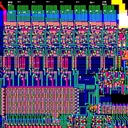
    Dieter M. aka "ttlworks" aus dem 6502.org Forum hat sich die GROSSE Mühe gemacht aus meinen Vektorbildern

    die Unterschiede zum 6502 mundgerecht herauszuarbeiten. Dafür hat er bereits einen Thread im 6502.org Forum eröffnet,

    den ich mit seiner Genehmigung hier nochmal reinkopiert habe! :thumbsup:


    Ich hoffe Euch gefällt es!


    Und nun möchte ich über das Thema "GATE IN" nix mehr falsches hören... :done:

  • This thread is about a transistor level dissection of what makes the 8501 different from the 6502,

    brought to you by Frank Wolf and ttlworks.


    The 8501 is a CPU introduced in 1984, manufactured in a HMOS-II process.

    It was used in the Commodore computers: C16, C116, Plus/4.


    Basically, it's a cousin of the 8500 (the HMOS variant of the 6510, used in the C64).


    The difference to the 8500 is,

    that the 8501 has 7 IO port pins (P0..P4, P6, P7),

    that the 8501 has a GATE_IN pin for latching the AEC signal,

    and that the 8501 has no NMI# pin.


    Writing to the P5 data Bit and data direction Bit has no effect.

    The P5 data Bit and data direction Bit always read back 0.


    The data bus drivers are disabled during IO port writes,

    means that during IO port writes, R/W# goes low, but there is no valid data on the bus.


    Note:

    for consistence with Frank's notation, low_active signals are named foo#, not /foo.


    Orientation for all the chip pictures: PHI2(out) is North.

  • My (ttlworks) Eagle 6.4 schematics for my schematic pictures in this thread,

    just in case if somebody needs them.


    Note: KiCad is supposed to be able to import these schematics,

    unfortunately it doesn't seem to be possible to disable the layers 'name' and 'value' in KiCad schematics,

    so making my schematics look nice and clean in KiCad will require some work, sorry.

  • 0) cheat sheet


    A very simplified schematic to give an overview about what came out during the dissection.


    A picture of the 8501 silicon, with the interesting areas marked according to the cheat sheet.


    Just as a reference, another picture of the 8501 silicon without the markings.


  • 1) Bias generator, located at the Nothern corner of the chip, between NMI# pad and IRQ# pad.


    Nothing fancy, basically a ring oscillator plus output driver.


    The 4 yellow boxes in the silicon picture labeled 'C' are small capacitors.


    The NMI# pad is present in the silicon, but the chip has no NMI# pin,

    this means that no wire is bonded to the pad.


    It looks like the NMI# trace is tacked to the output capacitor of the bias generator

    (the side of the capacitor which connects to the two FETs working as diodes)

    by using a pullup (pulldown ?) FET, and we have no idea why.


  • 2) AEC input buffer, located at the North West corner of the chip.


    Nothing fancy in there:

    AEC goes through three super buffers and becomes AEC_buffered.

    AEC_buffered has the same polarity as AEC:


    First super buffer is inverting, second is non_inverting, third is inverting.

    Means that the group of super buffers as a whole is non_inverting.


    There is a metal trace which connects to the output of the second (non_inverting) super buffer.

    It goes East, but it's dead because it's cut at the R/W# buffer.

    It probably was connected to the (low_active) output enable of the R/W buffer in a previous chip revision.

    We are getting there later when taking a look at the R/W# pad driver.

    //In the 6510, this connection probably isn't cut.


    BTW: in theory, HMOS-II is supposed to have a ca. 30ns propagation delay per logic gate when there is no bias generator.

    But since we have a bias generator on this chip, I'm not sure about those 30ns.


  • 3) GATE_IN logic, located South East on the chip, between GATE_IN pad and P7 pad.


    GATE_IN goes through two inverting super buffers and becomes GATE_IN_buffered.

    Means that GATE_IN_buffered has the same polarity as GATE_IN.


    GATE_IN buffered then controls a fully static transparent latch (as in "74373").

    The latch reads AEC_buffered, and gives out two signals:

    The non_inverted AEC_gated, and the inverted AEC#_gated.


  • 4) IO address decoder.


    ;---


    First, we have a 15 input NOR gate which checks A1..A15 to zero for identifying a read/write to IO address space.

    Except that the NOR gate doesn't instantly pop out when looking at the chip.


    What we really have on the chip is a long metal trace (labeled IO_SELECT) which runs at most of the West and South side of the chip.

    Each of the A1..A15 pad drivers has a FET which is tied to the metal trace, and pulls said metal trace to GND if the related address Bit is 1,

    but we are getting to the innards of the address pad drivers later.


    Also connected to the metal trace, we have a cute tiny pullup FET, located East of the A4,A5 pads, and it's hard to spot.


    The metal trace then goes to the input of a non inverting super buffer, which gives out IO_SELECT_buffered to the address decoder.

    Said buffer is located North of the GND pad. (GND pad is on the South edge of the chip).

    If the address points to $0000 or $0001, IO_SELECT_buffered is 1.

    si8501_4_io_select_pullup.png


    ;---


    Second, the address decoder logic is located North of the GATE_IN pad (GATE_IN pad is on the South edge of the chip).

    //North of the address decoder logic, we have the logic for the IO ports.


    At the West side of the address decoder logic we have two signals going in, IO_SELECT_buffered and A0#.

    A0# is low_active and tapped from the innards of the A0 pad driver, we are getting to it later.


    At the North side of the address decoder logic, we have the WRITE1 signal going in,

    that's the output of a transparent latch which is gated with PHI1 and samples the CPU_W/R# signal, we are getting to it later.

    Also, we have some output signals:

    WR_IO# is a low active signal for switching the IO data bus during writes.

    WR_0x00, RD_0x00, WR_0x01, RD_0x01 are high_active control signals for the IO port logic.

    OE_D# is the low active output enable for the D0..D7 data pad drivers.


    Note, that the D0..D7 data pad drivers are disabled during IO reads/writes.


  • 5) data read/write control, data read/write timing stuff that is.


    ;---


    The R/W# buffer is inverting, and it is fed with "internal_W/R#", we are getting later to this.


    The logic for generating "internal_R/W#" is made from three little parts, which have different locations on the chip:


    We have an AND gate (located west of the D4 pad driver) with PHI1 and GATE_IN_buffered at the inputs.

    The output of the AND controls a transparent latch (which is located South of the D2 pad driver).

    The latch samples CPU_W/R# and gives the signal to a lump of logic (which is located South of the D1 pad driver),

    said lump of logic contains an inverter followed by an inverting super buffer,

    which gives us "internal_W/R#" at the output.


    ;---


    For the rest, we have one block of logic which is located North from the P0 IO logic

    (West from the P0,P1 pad drivers, that is).


    CPU_W/R# is sampled by a transparent latch controlled by PHI1, generating WRITE1 for the IO address decoder.


    IO_SELECT_buffered (and the IO_SELECT_buffered# generated by an inverter) are sampled by transparent latches controlled by PHI1.

    The outputs of the latches are driving two tricky pulse shapers which generate two signals from PHI2:

    OE_IO_Data, high_active output enable for the read buffers in the IO logic for reading IO data into the CPU data input latch,

    OE_Data_in, high_active output enable for the read buffers at the D0..D7 data pads for reading the external data bus into the CPU data input latch.


    I would dare to say, that the purpose of these pulse shapers is to delay these two signals

    to make sure that the data read from the buffers fits the CPU read hold timing.


  • 6) R/W# pad driver, high up North on the chip.


    Nothing fancy.

    Inverting buffer with low_active output enable.


    Buffer inverts "internal W/R#" to external R/W.

    Output enable is the low_active AEC_#gated signal.


    Note the cut metal trace from AEC#_buffered to the R/W# pad driver output enable...


  • 7) D0 pad driver.


    Nothing fancy in there.


    D0 pad is driven by a non_inverting buffer (fed by D0_output),

    the (write) buffer has a low_active output enable OE_D#.


    D0 pad is read by an inverting buffer into the low_active D0_Data_in#,

    the (read) buffer has a high_active output enable OE_Data_in.


    7a) D3 pad driver.


    Since the D3 pad driver has a different layout than the D0 pad driver,

    I just wanted to know if both pad drivers have identical circuitry.


    They have.


  • 8) A11 latch + pad driver, down in the south of the chip.


    We have an inverter that turns A11_internal into the low_active A11_internal#.


    A11_internal# is sampled by a latch (three FET switches plus a non_inverting super buffer),

    controlled by PHI1, PHI2, and LD_ADDR.


    The low_active latch output goes to the A11 pad driver.

    Also, the low_active latch output goes into a super buffer.

    The high_active super buffer output goes to the A11 pad driver,

    also it goes to the gate of a FET that switches IO_SELECT to GND.


    Said FET is present in the A1..A15 logic, together with the IO_SELECT metal trace

    and one pullup resistor this gives us a 15 input NOR gate for detecting the IO address range

    $0000 and $0001, we already had mentioned this in 4) IO address decoder.


    Also, the address decoder taps into the inverted output of the A0 address latch,

    using the A0# signal to find out if the address is $0000 or $0001.


    The A11 pad driver has a high_active output enable: AEC_buffered.


  • 9) IO port.


    The IO port logic is rather compact, and west from the P1..P3 pad drivers.


    From North to South, we have the logic related to P1, P2, P3, P4, P6, P7,

    then the logic which makes the data Bit and data direction Bit for P5 zero during reads.

    //There is no P5 IO port in the 8501.


    //North from the IO port logic blocks we have data read/write control.

    //South from the IO port logic blocks we have the IO address decoder.


    P0 pad driver layout is a bit different from P1 pad driver layout, but the circuitry is identical.

    The P0 pad driver is nothing fancy.


    Note, that the ESD protection FET is not located close to the P0 pad.

    It's part of the P0 IO port logic block, which isn't optimal.

    My guess is that the designers did run out of space on the chips,

    and that unlike with the 6522 and 6526 the IO port pins of the 8501

    were not ment to give signals to the outerworld (outside of the computer).


    Looks like the IO port logic blocks were created by copy+paste,

    means the layout of all the IO logic blocks is more or less the same.

    So we only take a look at the P0 IO port logic.


    The low_active WR_IO# control signal puts the D0_output of the CPU on the IO data bus during peripheral writes.


    An inverting super buffer with a FET switch at the output controlled by the high_active OE_IO_Data signal

    puts the inverted data from the IO data bus on D0_data_in#.

    D0_data_in# also is fed by the D0 pad input buffer.

    D0_data_in# goes through a simple inverter before it enters the CPU as D0_data_in_latch.


    In the IO logic, we have two latches:

    WR_0x00 writes the P0 data direction latch.

    WR_0x01 writes the P0 data latch.


    The P0 input is sampled at PHI1 by a latch.

    Depending on if P0 is configurated as an input or an output,

    we have a multiplexer that either sends the output of the P0 latch to the IO data bus,

    or the output of the P0 data register.

    Connections at the multiplexer look a bit unusual,

    but I would say if a designer is paranoid about output pins of different chips working against each other,

    it seems to make sense.


    8501 has no P5.

    There is a block circuitry that forces the P5 data Bit and data direction bit to 0,

    and it looks like a normal IO block just was cut down to the bare minimum.